What's New in v5.4.12
2018.05.07
Improvements
What's New in v5.4.11
2018.04.25
Improvements
What's New in v5.4.10
2018.04.23
Improvements
What's New in v5.4.9
2018.04.20
Improvements
What's New in v5.4.7
2018.04.20
New Features
Improvements
What is new in v5.3.14
2018.03.21:
Improvement:
What is new in v5.3.12
2018.03.20:
New Feature:
Improvement:
What is new in v5.3.2
2018.03.07:
It is a big version upgrade, Easy do a lot of changes and improvements.
New Feature:
Improvement:
SHIFT key to batch selectWhat is new in v5.1.3
2018.01.22:
Improvement:
Forecast:
What is new in v4.11.9
2017.11.22:
Improvement:
What is new in v4.11.5
2017.11.17:
G(Avoid to close the Snap function by accidentally, that will make the wire to detach the PIN) and ctrl+shift+v(Invalid function).What is new in v4.10.3
2017.10.20:
Improvement:
What is new in v4.10.2
2017.10.17:
Improvement:
What is new in v4.10.1
2017.10.16:
New Feature:
Improvement:
Convert to PCB rather than Update PCB.What is new in v4.9.3
Local Auto Router
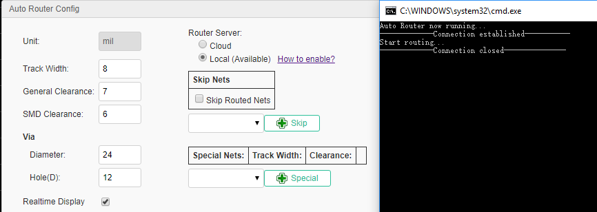
Before run the local auto router, you have to configure the browser, for more information please refer: PCB Layout - Route Tracks - Local Auto Router
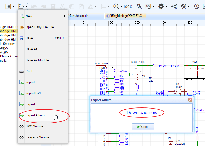
Export the Altium Designer file format
What is new in v4.8.5
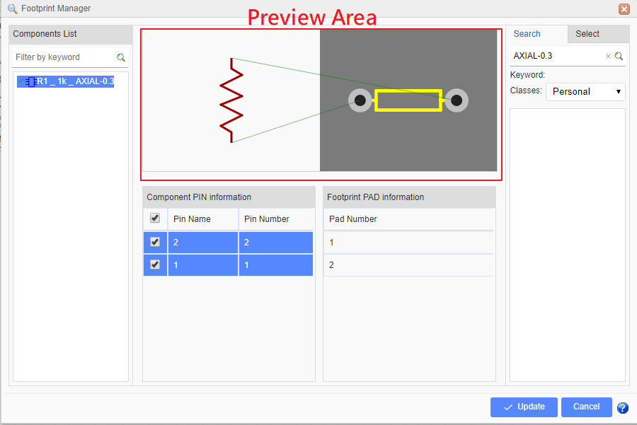
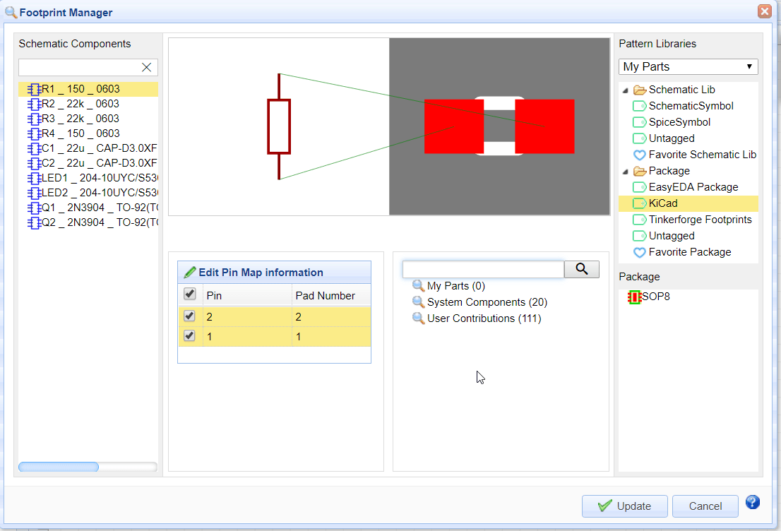
Footprint Manager Enhanced
1.Footprint manager will check your part's package correct or not automatically. If the part without the package or this package doesn't exist in EasyEDA Libraries, or if the part's Pins Number doesn't correspond the package's Pads Number correctly, the footprint manager will show the red alert.
Notice: If your schematic have many different packages, the footprint manager will take a few seconds to compare the packages' pads and your components' pins. Please wait for it.
2.In the preview area, you can zoom in, zoom out and pan with mouse.
LCSC Assembly Components
Buy Components From LCSC More Easily
We change the BOM export location in at LCSC.
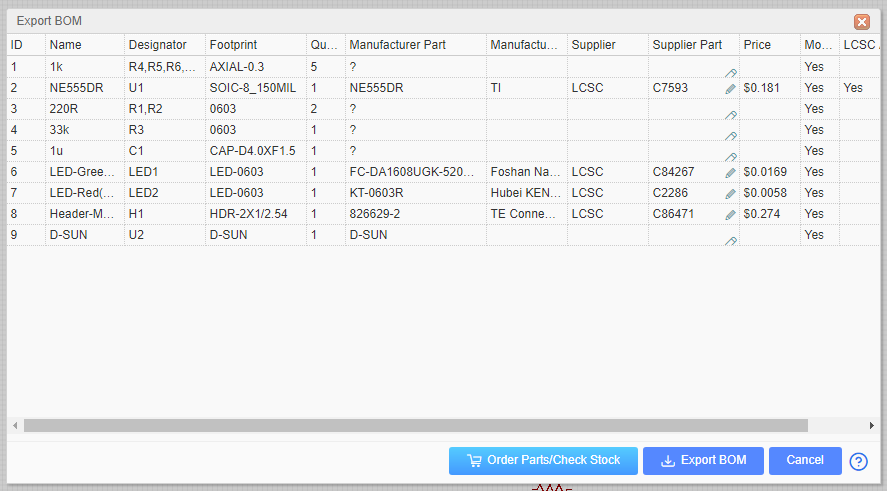
When you click "Export BOM at LCSC", we will help you to list all the components of your BOM, and you just need to put them to the cart and check out.
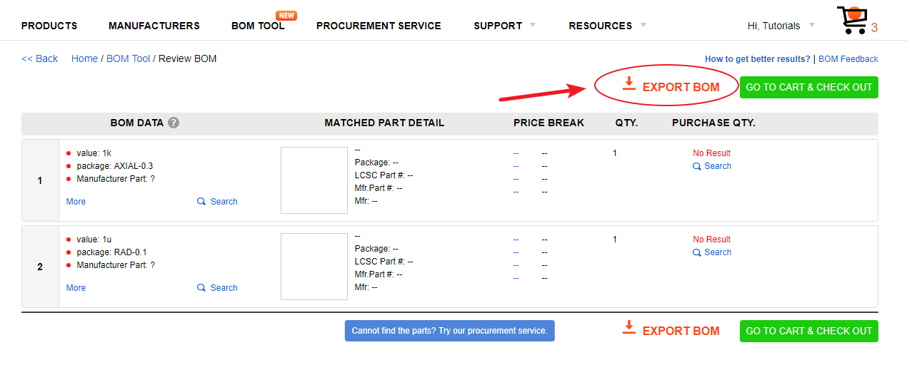
And Click the "BOM"button to download the BOM file.
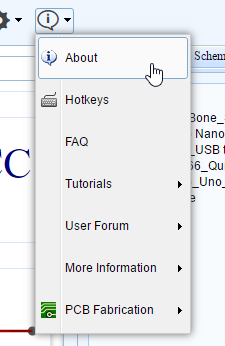
Documents Tab Switch
Protractor
What is new in v4.6.4
New Footprint Manager
New Arc tool
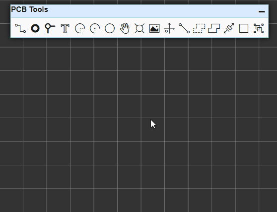
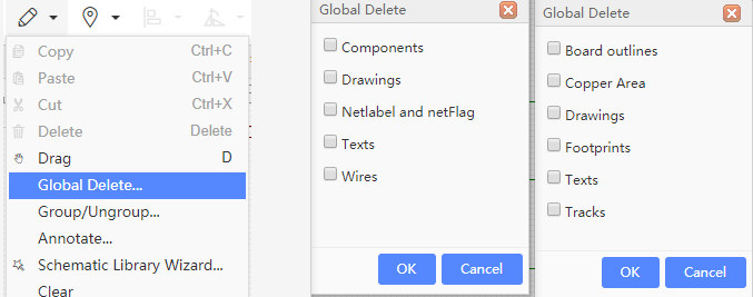
Global Delete
Move selected component
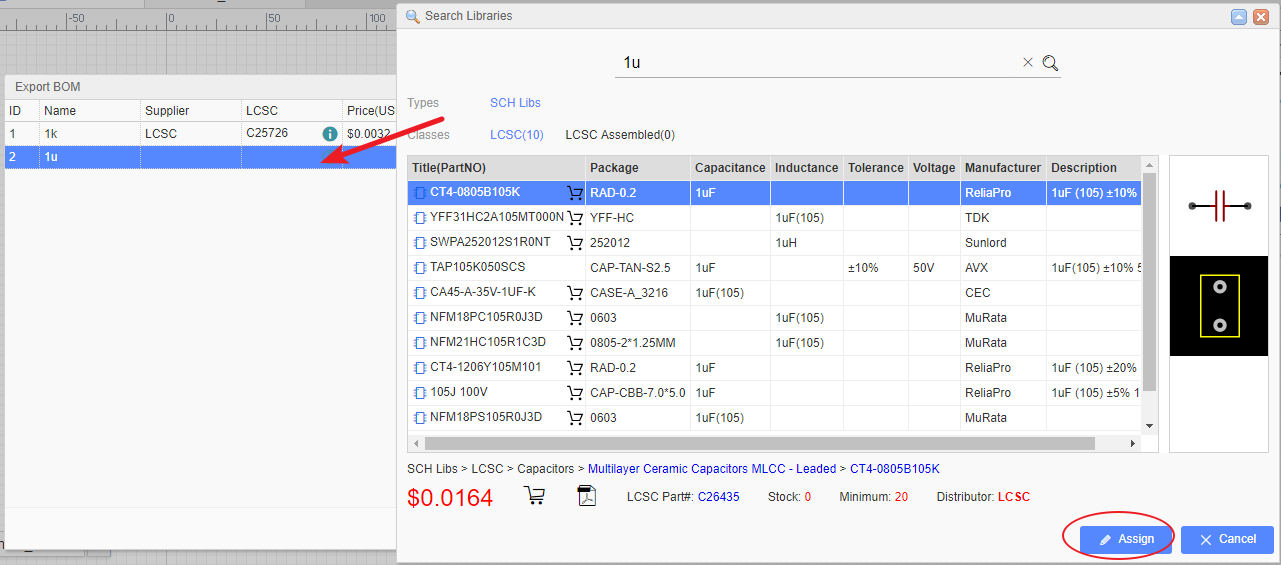
BOM export on the top toolbar
![]()
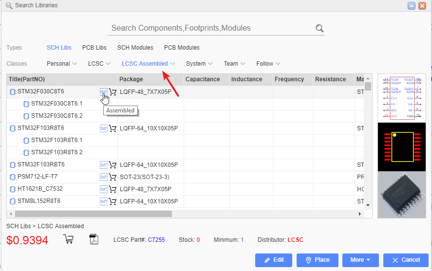
In the BOM export dialog,you can assign LCSC part's order code for your components.
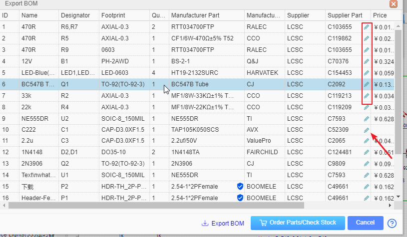
After clicking on the assign icon,the components and packages search dialog will open in which you can choose the component that you want to assign.
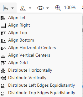
More Align options
Import enhance
New Altium Design Import
It is faster and better, and it support big files. Please make sure that you save the file as ASCII before importing.
Better DXF Import
Importing DXF file to PCB is better.
What is new in the V4.5.6
After 7 years of development, EasyEDA are pleased to announce the new version: V4.5.6. which introduces many new features. Try it at https://easyeda.com/editor
New UI
Before V4.5, EasyEDA's UI is not professional, now we redesign the icons and theme.
LCSC
EasyEDA partner with China’s largest electronic components online store by customers and ordering quantity launch https://lcsc.com.
Cross Probe in Schematic and PCB
This tool is used to cross probe from chosen objects on the current schematic to its corresponding counterparts in the PCB, or from PCB Footprints to corresponding counterparts in the schematic.
Note, you need to open the schematics and PCB. Don't forget to use hotkey SHIFT+X
Thanks to this topic https://easyeda.com/forum/topic/TAB_to_toggle_between_PCB_amp_schematic-LDdaKIigs
Board outline wizard
Some users want to set very precision board outlines, now we can do in this way. Open your PCB, find the menu via toolbar.
Then you can see such a dialog.
In this dialog, we provide 3 type board outline setting, Rectangular , Circular, Round Rect.
If you need other complex board outline, you can import a DXF file.
Change Supper Menu position
In old version, the supper menu is a bit litter hard to find, now we set it at a good place.
New Design Manger
The old design manager is hard to find too, now we move it to the left panel.
We hope you enjoy the new version!
And as always, if you have any questions or suggestions, do let us know. [email protected]
What is new in the V4.1.1.X
After 7 years of development, EasyEDA are pleased to announce the new version: V4.1.1. which introduces many new features. Try it at https://easyeda.com/editor.
2017 Spring Festival Notification
Please check this link 2017 Spring Festival Notification
EasyEDA ambitions in 2017
1. Provide components ordering with your PCB.
So you can not only order your PCB from us; you will also be able to order many common components directly from us. We will ship the components with your PCB so saving you lots of time and money because there's no need to hunt for components and compare pricing from big name suppliers.
2. Provide PCB assembly service.
For a long time, EasyEDA has been able to provide a PCB assembly service but up to now just a few customers who chat with us via email know about this service. In 2017, we will make this service public. So after you design the PCB, we will not only help you to source the components but we will kit and assemble them onto your PCB before shipping the completed PCBs to you. That way, you can focus more of your time and effort into the design and debug tasks.
New EasyEDA libs
From this version, we have changed the EasyEDA Libs to try make it easier to find, place and order components and to make schematic conversion to PCB simpler. Placing any component from the EasyEDA Libs into a schematic will therefore also automatically complete the PCB package and all the required BoM information fields.
For Resistor, Capacitor, Inductor symbols, EasyEDA now provides the components with package selection and provides dedicated US styles and IEC styles
For other common parts such as discretes and ICs, we now provide symbols for components with specific packages and which can be ordered from EasyEDA.
For the Connector section,
EasyEDA now provides Header-Male, Header-Female, Screw Terminal, IDC box, RJ45, RJ11, USB and audio interface. All of these components can be ordered straight from EasyEDA with your PCB.
Note however that this is a big change from the earlier versions of the EasyEDA Libs because from V4.1.1 most of the non-passive components in the EasyEDA Libs will no longer have spice models attached to them.
Schematic symbols with spice simulation models attached to them can now be found using the More Libraries... button (or SHIFT+F) under System Components > Spice Simulation
So, you do need to spend some time to explore these changes.
Images for EasyEDA components.
Sometimes, it can be hard to visualise what a component really looks like just from package or schematic symbols, so now we provide real product images, photographed against a 1mm grid for reference,
Work as a team
Before EasyEDA version V4, if you wanted to work together with your partners, you had to use the Add Member function.
Access Control has lots of limitations on who can create projects, schematics and PCBs and more importantly, when you try to convert your schematics to PCB, you may find that some packages create error messages which can be hard to track down.
Now EasyEDA provides a new team feature with which you can work seamlessly with your partners. You can work as if everyone is logged in under the same account, with full access to all components, Schematics, PCBs and Projects.
How to find the team function.
Under the dashboard , there is a team section.
How to create a team.
There is a link as shown in the image above, or click this link after you login.
How to switch to team model.
1) switch in the dashboard.
After you have created a team, click the team name and the dashboard will switch to showing only the team projects, files and components.
After switching to a team, there is a team management section where you can manage your team members, invite new team members and even delete the team.
2) switch in the editor.
Under your personal menu, there is a sub menu allowing you to switch to a team or to your personal account.
How to Upgrade to a team
If you want to contribute all of your designs to a team, you can use this function. First you need to create a team, then click the link, shown below, under dashboard.
Be careful with this function because after you do that, all of your components, projects will be moved to your team.
Tips about the team function.
Warning
After you modify a PCB, please remember to rebuild the copper area before placing the final PCB order.
In a few weeks time, we will introduce the feature that EasyEDA will force you to rebuild the copper area before placing the final PCB order but for now you need to remember: Easyeda does not rebuild the copper area automatically for you before placing your order.
Desktop Version beta version
A download link for this will be available soon.
We hope you enjoy the new version!
And as always, if you have any questions or suggestions, do let us know.
What is new in the V3.10.X
The new version EasyEDA, V3.10.x. introduces lots of new features. Try it at https://easyeda.com/editor.
Better Mac User Experience
Please note that when running EasyEDA on a Mac, for the best user experience, we recommend using Chrome instead of Safari.
1. Pan
When Using the Mouse
Hold down the right click and move your mouse and the canvas will pan with the cursor.
Before using the Magic Mouse, you need to enable the right click function via this video. https://www.youtube.com/watch?v=ekzIoAxXSHE,
SHIFT key then move a single finger: the canvas will pan horizontally.CONTROL key then move a single finger: the canvas will pan vertically. 2. Zoom
When Using the Mouse
Scroll the middle button of the mouse (or Magic mouse).
When Using the Touchpad
Sliding a single finger up zooms in and sliding down zooms out.
New Pad attribute.
New Slot and Plated attributes have been added for the hole in a pad as illustrated in the image below
Components
The component search function has been significantly improved to make finding part symbols and footprints quicker and easier. Press hot key SHIFT+F or click it via toolbar
In the new components dialog, it is easy to select the right components via tags and you can set tags for your own components.
New Dialog
When creating a schematic lib, there is an input dialog for entering sourcing information, such as supplier information, supplier part number and datasheet. Information can be added at the time the schematic lib is created or these steps can be skipped at this stage and add these later.
New Component attribute
The new version of EasyEDA adds a Mounted attribute at the component, to simplify the identification and kitting of optional components which may be fitted in one assembly but not in another. This attribute can be set to YES to list the part in the BoM. If the Mounted attribute is set to NO as illustrated in the image below then the part will not be listed in the BOM.
Components search dialog
If the EasyEDA Components option is selected, then a dialog opens as illustrated in the image below.
EasyEDA team has spent a lot of time to build these EasyEDA Components components and packages and we recommend them as preferred components, because the packages have been carefully checked and verified, the footprints have been designed for reliable soldering by our PCB manufacturing and because these components can all be ordered directly from EasyEDA.
There are several other categories to explore but these components may need more carefully checking or may be a little harder to source.
New search filter
When updating a package, using new filter terms, it is now possible to search only for a symbol or only for a package/footprint. For example in the filter entry below:
AXIAL doctype:pcb
the filter term:
doctype:pcb
will just search for a PCB package with the name AXIAL.
Similarly, the filter term:
doctype:sch
will just search for components (symbols) without listing packages.
Synchronous schematic and PCB
Converting a schematic to PCB can be done using the Convert Project to PCB... button as illustrated in the toolbar below but a new update PCB button has been added so that modifications to the schematic can immediately be passed forward to update the a selected PCB without having the PCB editor window already open.
Add Frame
It is now possible to add design notes to the frame and the frame selection, for example A4, can assist in aligning and improve the look of printed schematics and PCB designs.
click the frame button like bellow image
As illustrated in the image below:
the bottom right zone can be selected and dragged or the frame can be dragged and deleted.
Hide the simulation button
EasyEDA's simulation function is powerful but it is not easy to use. Many of our users run a schematic which, for example, may include symbols or blocks - such Wifi modules, MCU, DSP and ADC devices - for which no simulation models exist. This can be very discouraging and frustrating, especially for users that are new to simulation and - because it is a CPU intensive task - at the same time can also waste lots of CPU resource at the expense of other tasks such as autorouting and rendering on larger PCBs.
To reduce the casual use of simulaton we have taken the decision, not to remove it but to simply hide the simulation button from the tool bar. Simulations can still be constructed and saved exactly as before but they can now only be run using the CTRL+R to run the simulation and we strongly recommend first studying - and trying out the many examples in - the EasyEDA Simulation eBook.
Desktop version coming soon
EasyEDA will provide a desktop version for offline use.
We hope you enjoy the new version!
And as always, if you have any questions or suggestions, do let us know.
What is new in the V3.2.X
The new version is V3.2.x. EasyEDA has lots of new features in the version. Try it via https://easyeda.com/editor.
Invite Friends to Win a Gift
If you like to help your friends to use this nice web based EDA tool, you can invite him/her to join EasyEDA. At the same time, you and your friends will get a $5 coupon to order PCB from EasyEDA. Why not to give this feature a try?
Click this link invite your friends now
Version History
It is easy to get this fundtion, right click the document which you need to find it's version like bellow image
After clicking the history version link, you will get a list of all of the versions like bellow image.
click the version number, you can open the saved file on the editor, if this is what you need, you can save it to your project and delete your bad file.
Note:
Auto Router
For some simply or prototype PCBs, you may want to use the auto router function to save time. Layout is a time cost and dull job. EasyEDA spends lots of time to provide such featureand loved by our users.
Steps:
Ripup NetsGND net, you can skip the GND net.Insert Image/Logo to PCB
On PCB and PCB Lib editor, there is a new feature on the PCB Tool bar like the bellow image.
After click it and select the image, you will goto bellow image.
In this dialog, you can choose your favorite image, EasyEDA support jpg, BMP, 'PNG, 'GIF, and SVG. not likes some other EDA tools, they just support a Monochrome Bitmap image, EasyEDA support full color. but Monochrome Bitmap is welcome.
You can adjust the tolerance and reset the image size at there.
The image will be inserted to the active layer, if it is not right, you can change the attribute of it. Such as TopSilkLayer.
More Fonts for PCB
From V3.2.x, You can add more fonts from your computer or download some free fonts .
Select the text, then you can find a Font-family attribute on the right panel like bellow image.
Click the add button, then choose the font, the font file must be ttf or otf.
So you can add any fonts by your self. EasyEDA desn't cache the font on our server, so if you close the editor, you need to add the font again by your self.
Note:
If you use the other font, the LineWidth attribute is useless, because it will be auo by change the Height.
Change Attributes in Batch on PCB Editor
Some times, we need to change some attributes in the same together, such as the track width, hole size and font size.
Now, you can select them and do some changes. Taking the track for an example. If you select 3 tracks, now you can change their Width, Layer, Net together.
Other items such as Pad, Via, and TEXT, you can try to play this feature.
New Track Style
When routing, some time we need to add an Arc segment, or change the inflection direction. Now we can do this easily.
Change to Arc style, You can use Hot key L to toggle from 45 degree to Arc.
You can change inflection direction when router, from A to B, we have two ways.
When you router from A to B, the default track is 1, but if you press Space bar key, the track will be changed to 2.
Modules
Copying codes is an easy job for coders, now copy and reuse a schematic or PCB are easy now.
Take a power supply unit for example, you can save this unit as a schematic module.
After saving, you can find it at the module section. And you can place the whole block to your schematic.
Get a Invoice After PCB Order
For company users, after order PCB, they may need an invoice, you can find it at .
History orders. There is an invoice link, you can open it and save it as pdf or html file.
Contribute Your Symbols and Package to EasyEDA
Right click your parts, you can share symbols and package to EasyEDA system libs, then, every one can use them as their own parts.
Delete a Segment from a Track
In lots of other EDA tools, the track is segment line, but in EasyEDA, the track is polyline. some time, if we want to delete a segment, we must delete the whole track and router again. Now we provide a not bad way to do this. Moving your mouse to the segment which you want to delete, click it, then hold the SHIFT and double click it. the segment will be removed.
Change Cursor Style
Some users don't like the cross cursor, so you can change it to arrow cursor like bellow image.
Better Navigation Bar for Components.
On How To Find The Schematic Libraries, you can find a way to use many many components and package, now EasyEDA provide a great navigation bar on the top. You can use some open source parts and Pololu Module , like bellow image.
Enjoy it, if you have any questions, do let us know.