

Hello!
So I am trying to do a faceplate using text and graphics, exposing copper in a PCB, and I have some issues (and lack of knowledge).
I found this topic ([https://easyeda.com/forum/topic/expose-coper-of-text-object-8a343e5137464bf997da75568d7ff2e7](https://easyeda.com/forum/topic/expose-coper-of-text-object-8a343e5137464bf997da75568d7ff2e7)) and this is what I did:
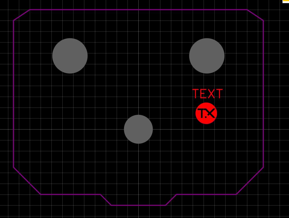
1- the faceplate is this, three holes for potentiometers (grey ones) and outlines in purple. The text and symbol I am testing:
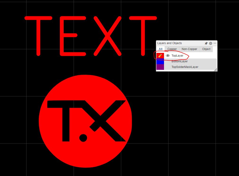
2- so I added 2x copies of each text AND graphic. One of each to "Top Layer":
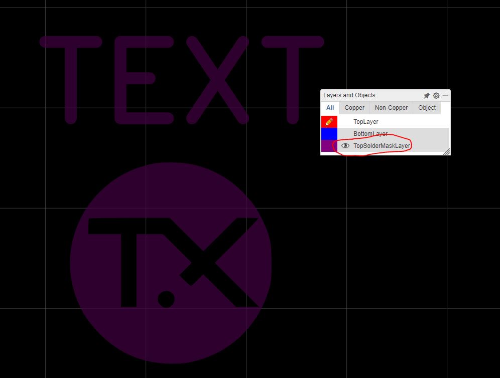
3- and the other on "Top Solder Mask Layer":
<br>
Now the question is, what do I do next??
Mind that this is not a "electronic schematic", it's just a design. Should I add a "net" (GND for example)????
Thank you for your help!

